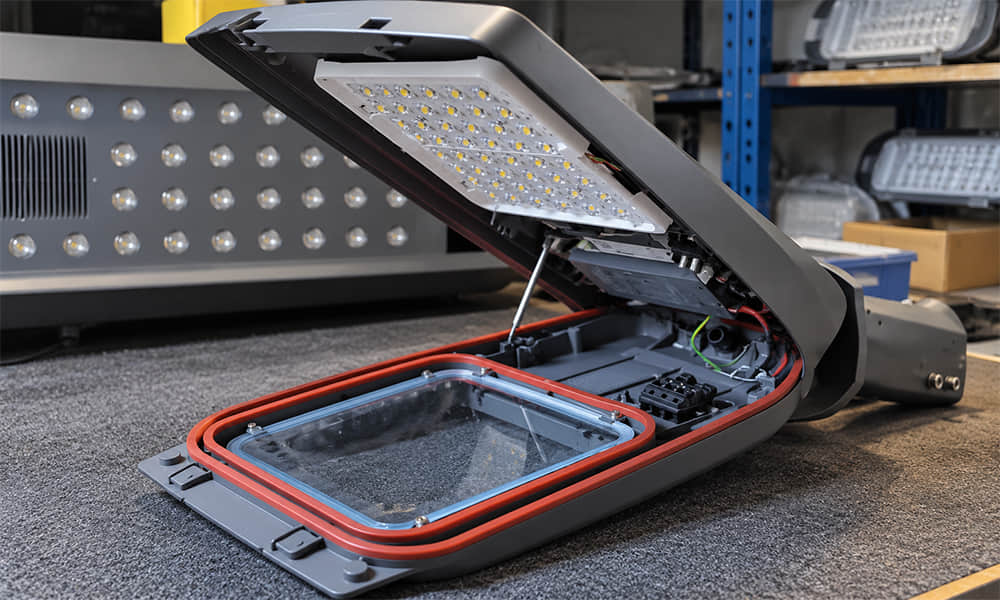
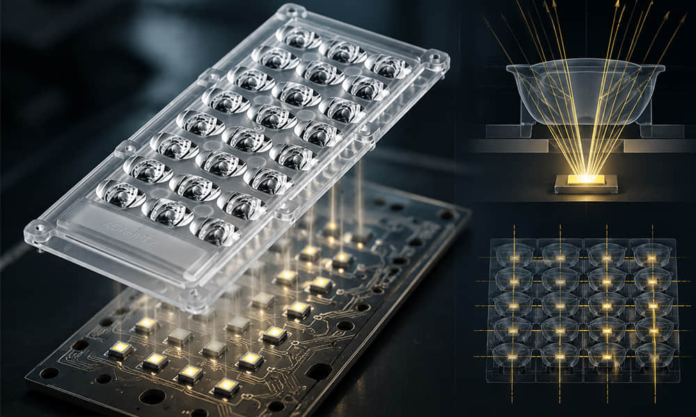
Matching an LED lens to a PCB layout requires more than checking the overall lens size and number of LEDs. The LED package, array pitch, optical centre, LED-to-lens distance and mounting structure must all correspond with the optical design.
A lens may fit inside a luminaire mechanically but still produce an unsuitable beam. If the LED is not aligned with the optical centre of the lens, the distribution may shift, become distorted or lose its intended cutoff characteristics. In a multi-lens array, even a small difference between the LED pitch and lens pitch can affect every optical cell.
This guide explains how to match an LED lens to a PCB, how to evaluate LED package and array compatibility, and how to determine whether an existing lens can be used with your PCB layout.
Why the PCB Is Part of the LED Optical System
A printed circuit board is commonly treated as an electrical and thermal component. In an LED luminaire, however, the PCB is also part of the optical system because it determines the position of every light source relative to the lens.
The PCB controls:
- The number of LEDs in the luminaire;
- The horizontal and vertical distance between LEDs;
- The shape and orientation of the LED array;
- The position of each LED relative to its optical cell;
- The location of screws, locating pins and mounting holes;
- The available mechanical space for the lens;
- The relationship between the lens, gasket and luminaire housing;
- The height of the LED emitting surface relative to the optical lens.
A suitable PCB layout for an LED lens keeps every light source in the position assumed during optical simulation. If the LED moves away from this position, the manufactured luminaire may produce a different light distribution from the original design.
This is particularly important in street lighting, sports lighting, high-bay lighting and other applications that require controlled beams. A small change in LED position can affect forward throw, lateral spread, cutoff, glare and illumination uniformity.
The PCB, LED and lens should therefore be evaluated as one optical assembly. Selecting each component separately and combining them at the end of development can create unexpected mechanical and photometric problems.
How to Align the LED Optical Centre with the Lens Centre
What Is the LED Optical Centre?
The LED optical centre is the effective position from which the lens receives light. It is related to the LED's light-emitting surface, internal chip structure, phosphor area and primary optical design.
The optical centre is not always identical to the geometric centre of the external package. Two LEDs with similar external dimensions may use different internal chip layouts or light-emitting surface sizes.
This is one reason why a lens developed for one 5050 LED should not automatically be assumed to work with every 5050 LED. The package name describes its approximate external size, but it does not define every internal optical characteristic.
What Is the Lens Optical Centre?
Each optical cell in an LED lens has a designed reference point and optical axis. During optical simulation, the LED is placed at a controlled position relative to the refractive and total-internal-reflection surfaces.
For a symmetric lens, the optical axis may be close to the physical centre of the component. For an asymmetric roadway lens, the surfaces intentionally redirect light away from the centre. Even in an asymmetric design, the original LED position remains essential to achieving the intended distribution.
What Happens When the LED and Lens Are Misaligned?
Correct LED lens alignment allows light rays to enter the designed optical surfaces at the expected positions and angles.
If the LED is laterally displaced, the result may include:
- A shifted beam direction;
- Uneven intensity on opposite sides of the distribution;
- A change in the maximum candela direction;
- Reduced cutoff control;
- Increased backlight or spill light;
- Distortion of a symmetric or asymmetric pattern;
- Reduced consistency between luminaires.
The acceptable LED position tolerance depends on the lens design, LED package and target beam. A narrow beam or sharply controlled cutoff optic may be more sensitive to displacement than a broad general-lighting lens.
There is no universal alignment tolerance that applies to every LED lens. The acceptable range should be established through optical simulation, mechanical drawings, sample assembly and photometric testing.
How LED Package Size Affects Lens Compatibility
LED packages such as 2835, 3030, 3535, 5050 and 7070 differ in more than their external dimensions. Their light-emitting surfaces, package heights, internal chip structures and primary optical features may also differ.
Important LED package characteristics include:
- Overall package length and width;
- Size and shape of the light-emitting surface;
- Phosphor position;
- Package height;
- Flat or domed primary optics;
- Single-chip or multi-chip construction;
- Native emission pattern;
- Operating current and thermal behaviour.
The size of the light-emitting surface is especially important. A lens designed around a relatively small source may produce a less controlled distribution when it is used with a larger emitting surface.
The change may cause:
- A wider beam;
- Lower peak intensity;
- A softer cutoff boundary;
- Reduced colour mixing;
- Changes in an asymmetric distribution;
- More light leakage around the optical cavity.
A larger package may also interfere mechanically with the lens cavity or support structure. Conversely, a smaller LED may fit inside the cavity but sit at an unsuitable height or position.
When checking LED package lens compatibility, engineers should review the complete LED datasheet. The general package name alone is insufficient for final approval.
Why LED Pitch Must Match the Lens Pitch
LED pitch is the centre-to-centre distance between LEDs on a PCB. Lens pitch is the centre-to-centre distance between the corresponding optical cells in a multi-lens array.
For correct alignment, the LED pitch and lens pitch must match within the specified production tolerance. If they do not match, the first LED may appear correctly centred while the alignment error becomes progressively larger across the array.
This accumulated error is especially important in long or high-density arrays. A small pitch difference repeated across 12, 24 or more LEDs can create a significant displacement at the far end of the module.
Array Format Does Not Guarantee Compatibility
Descriptions such as 2×2, 2×3, 2×6 or 3×8 explain the general LED arrangement, but they do not guarantee that a lens will match a PCB.
Two products described as 2×3 arrays may use different horizontal and vertical pitch dimensions. Their mounting holes, locating pins and overall dimensions may also be different.
Engineers should compare:
- Horizontal LED pitch;
- Vertical LED pitch;
- Overall array dimensions;
- Distance from the LED array to the PCB edge;
- Mounting-hole coordinates;
- Lens locating pins and support legs;
- Orientation of the first LED and optical cell;
- Component keep-out areas around the array.
Example: 50 mm 2×3 LED Lens Array
Asahi's 50 mm 2×3 LED lens series contains six optical cells in a compact module. The series includes different beam options for flood, area and street lighting.
The array description and overall size provide an initial reference, but the PCB still needs to be checked against the actual LED pitch, optical centre coordinates and mounting features.
Example: 173 mm 3×8 LED Lens Array
The 173 mm 3×8 LED lens series includes larger integrated 24-LED options.
In a 24-cell array, cumulative pitch error becomes more important because the alignment must be maintained across the full module. The PCB drawing should be overlaid with the lens drawing before samples are ordered or the PCB enters production.
For a broader explanation of optical arrays, read What Is a Multi-Lens Array?
How LED-to-Lens Distance Changes the Beam
The vertical distance between the LED and lens is another critical matching parameter. Optical surfaces are calculated around a defined source position. Moving the source upward or downward changes the angles at which light enters those surfaces.
An incorrect LED-to-lens distance may cause:
- A wider or narrower beam;
- A change in maximum luminous intensity;
- A shift in beam direction;
- Reduced optical efficiency;
- Light leakage around the optical cavity;
- A blurred cutoff boundary;
- Changes in an asymmetric distribution;
- Increased variation between samples.
The final distance is affected by more than the nominal lens height. The complete assembly stack must be considered.
Relevant dimensions include:
- PCB thickness;
- LED package height;
- Solder thickness;
- Lens support-leg height;
- Gasket thickness;
- Screw position and mounting pressure;
- Protective glass or cover position;
- Luminaire housing tolerance.
The term “focal distance” is sometimes used informally when discussing LED lenses. However, many modern freeform and TIR optics do not behave like simple imaging lenses. The correct LED position should be defined by the optical design and mechanical drawing.
How PCB and Lens Mounting Tolerances Affect Light Distribution
A prototype may produce the target distribution while mass-produced luminaires show variation if PCB, LED, lens and housing tolerances are not controlled.
LED Placement Tolerance
Surface-mount equipment positions LEDs according to the PCB coordinates, but every assembly process has an allowable placement range. Lateral displacement and rotational error may affect the relationship between the LED and optical cell.
Rotation may be relevant for LEDs with a non-uniform internal chip layout or for optical systems in which LED orientation is specified.
PCB Dimensional Tolerance
PCB manufacturing can introduce variation in overall dimensions, mounting holes and circuit features. The mechanical reference used to position the lens should be accurately related to the LED coordinates.
If the PCB is located by one set of housing features and the lens is located by another, the tolerances of both positioning systems may accumulate.
Lens Mounting Tolerance
Locating pins, screw holes, support legs and sealing gaskets control how the lens sits above the PCB. Loose positioning features may allow lateral movement, while uneven screw pressure can tilt or deform a large lens.
The mounting design should position the lens repeatedly without placing excessive stress on the optical surfaces.
Accumulated Assembly Variation
A small LED placement error, PCB-hole deviation, lens shrinkage and housing tolerance may each appear acceptable when considered separately. When combined, they can move the LED significantly away from its intended optical position.
Tolerance analysis does not attempt to eliminate all manufacturing variation. Its purpose is to define acceptable limits that preserve light distribution and photometric consistency throughout production.
Why the Same Lens Can Produce Different IES Files
An IES file represents a specific tested or calculated optical configuration. It does not represent an isolated lens under every possible LED and assembly condition.
The same lens may produce different IES results when there is a change in:
- LED manufacturer or model;
- Light-emitting surface size;
- LED package height;
- LED operating current;
- LED position or rotation;
- PCB array pitch;
- LED-to-lens distance;
- Lens material or surface condition;
- Protective glass or diffuser;
- Luminaire assembly and internal reflection.
A catalogue IES file can support initial evaluation when the intended assembly is sufficiently similar to the tested configuration. Final validation should use the actual LED, PCB and luminaire structure.
To understand how to evaluate this data, read How to Read an IES File for LED Street Light Lens Selection.
Can an Existing LED Lens Fit a Custom PCB?
An existing lens can often be used with a customer PCB, but compatibility must be evaluated systematically. Mechanical fit alone is not sufficient.
Step 1: Confirm the Exact LED Package
Review the LED manufacturer, model, package dimensions, emitting surface and height. Do not approve compatibility using only a general label such as 3030 or 5050.
Step 2: Check the LED Array Format
Compare the number of LEDs and their arrangement. A 2×3 lens requires six corresponding light sources, but the horizontal and vertical pitch must also match.
Step 3: Compare LED and Optical Coordinates
Overlay the PCB LED coordinates with the optical-cell centres. This is more reliable than comparing only the overall PCB and lens dimensions.
Step 4: Review Mounting Features
Check screw holes, locating pins, support legs, PCB edges, connectors and other electronic components that may interfere with the lens.
Step 5: Confirm the Vertical Position
Calculate the actual distance between the LED emitting surface and the lens reference. Include the PCB, LED package, gasket and mounting structure.
Step 6: Evaluate the Required Light Distribution
Mechanical compatibility is useful only if the lens provides an appropriate beam. Review the available IES file and compare it with the target application.
Step 7: Assemble and Test Samples
Use physical samples to confirm assembly, sealing and photometric performance. If the complete luminaire differs from the original tested configuration, new photometric testing may be required.
A structured LED lens compatibility check can reduce development time and avoid unnecessary optical tooling when an appropriate lens is already available.
Should the PCB or the Lens Be Modified?
When an existing lens and PCB do not match, the project team must decide whether to modify the PCB or develop a new lens. The better option depends on the development stage, expected volume, performance target and available schedule.
When Modifying the PCB May Be Better
PCB modification may be more efficient when:
- The project is still in an early design stage;
- An existing lens already provides a suitable distribution;
- Only LED positions or mounting holes need adjustment;
- Changing the PCB costs less than developing new optical tooling;
- The development schedule is short;
- The expected production volume does not justify a dedicated mould.
In this situation, the PCB can be developed around a proven optical platform. This may reduce technical risk and shorten the sampling process.
When Developing a New Lens May Be Better
A new optical lens may be appropriate when:
- The PCB has already been finalized;
- The LED coordinates cannot be changed;
- The luminaire housing or sealing structure is fixed;
- No existing lens provides the target distribution;
- The project requires special cutoff or backlight control;
- The expected volume supports optical mould investment;
- The customer requires an independent optical platform.
The decision should consider optical performance and total project cost rather than tooling price alone. A properly matched lens may improve target-area coverage, reduce wasted light and help the luminaire use LED output more effectively.
What Files Are Required for an LED Lens Compatibility Check?
Complete input files help an optical manufacturer evaluate the LED lens and PCB matching conditions efficiently.
Recommended information includes:
- LED manufacturer and full model number;
- LED datasheet;
- PCB 2D drawing;
- LED centre coordinates;
- Horizontal and vertical LED pitch;
- PCB outline and thickness;
- Mounting-hole coordinates;
- Connector and component keep-out areas;
- Luminaire assembly drawing;
- Available 3D files;
- Maximum available lens dimensions;
- Existing IES file;
- Target IES distribution or simulation result;
- Application and installation conditions;
- Material and sealing requirements.
A PDF drawing may be sufficient for an initial review. Editable 2D and 3D files are generally more useful when structural modification or a new optical component is required.
What Happens After an LED Lens and PCB Compatibility Review?
1. LED and PCB Review
The optical team reviews the LED package, array coordinates, PCB dimensions and available installation space.
2. Existing Lens Search
Available products are compared with the PCB and target distribution. If an existing lens appears compatible, technical data and samples can be prepared for evaluation.
3. Sample Fit Evaluation
Samples are assembled with the target PCB to verify LED position, mounting features, sealing space and mechanical interference.
4. Photometric Evaluation
Available IES data can be used for preliminary simulation. A complete luminaire test may be needed when the LED, PCB or assembly differs from the original configuration.
5. Optical Development When Required
If no existing lens matches the PCB and target distribution, Asahi can provide custom LED lens design based on the actual LED package, PCB coordinates and luminaire structure.
6. Structure and Tolerance Review
Optical surfaces are integrated with mounting holes, locating pins, support legs, sealing areas and production tolerances.
7. Mould, Samples and Production
After the design is approved, the project can proceed through optical mould development, sample production, photometric testing, trial production and mass production.
Learn more about Asahi's LED optical design capabilities.
Send Your PCB for an LED Lens Evaluation
If you already have a PCB layout, Asahi can check whether an existing lens matches the LED package, array pitch, available dimensions and target light distribution.
Send your LED datasheet, PCB drawing, LED coordinates, luminaire structure and target IES requirements. Our optical team can determine whether:
- An existing lens can be used directly;
- The PCB should be adjusted to match an existing optical platform;
- A physical sample test is required;
- A new optical lens should be developed.
Send Your PCB for Lens Evaluation
FAQ About LED Lens and PCB Matching
Q: Can any LED lens be used with any PCB?
No. The LED package, array format, LED pitch, mounting-hole positions, LED-to-lens distance and target light distribution must match the lens design. A lens may fit mechanically but still produce an unsuitable beam.
Q: How much LED misalignment can a lens tolerate?
There is no universal tolerance for every lens. The acceptable displacement depends on the LED package, optical structure, beam type and performance target. Narrow beams and sharply controlled optics may be more sensitive. Tolerance should be confirmed through simulation and testing.
Q: Can the same lens work with both 3030 and 5050 LEDs?
Some lens families support multiple LED packages, but compatibility must be checked for the exact LED model. The emitting-surface size, package height and internal structure may change the beam even when both LEDs fit mechanically.
Q: Can Asahi recommend a lens from a PCB drawing?
Yes. Asahi can review the PCB dimensions, LED package, LED coordinates, mounting structure and target distribution to identify possible existing lenses. Samples and photometric data can then be used for further evaluation.
Q: When is a new optical lens mould required?
A new mould is normally required when no existing lens can match both the PCB layout and target optical distribution. It may also be appropriate for high-volume projects that require an independent lens structure, special sealing features or proprietary photometric performance.